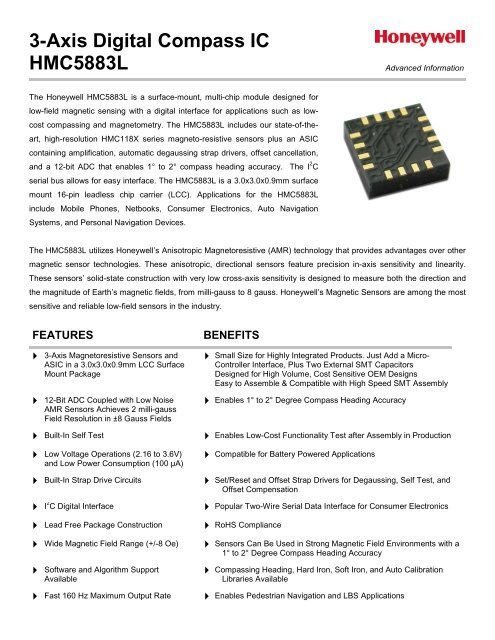
Three-Axis Digital Compass IC HMC5883L
Three-Axis Digital Compass IC HMC5883L
Three-Axis Digital Compass IC HMC5883L

Create successful ePaper yourself
Turn your PDF publications into a flip-book with our unique Google optimized e-Paper software.
3-<strong>Axis</strong> <strong>Digital</strong> <strong>Compass</strong> <strong>IC</strong><br />
<strong>HMC5883L</strong><br />
Advanced Information<br />
The Honeywell <strong>HMC5883L</strong> is a surface-mount, multi-chip module designed for<br />
low-field magnetic sensing with a digital interface for applications such as lowcost<br />
compassing and magnetometry. The <strong>HMC5883L</strong> includes our state-of-theart,<br />
high-resolution HMC118X series magneto-resistive sensors plus an AS<strong>IC</strong><br />
containing amplification, automatic degaussing strap drivers, offset cancellation,<br />
and a 12-bit ADC that enables 1° to 2° compass heading accuracy. The I 2 C<br />
serial bus allows for easy interface. The <strong>HMC5883L</strong> is a 3.0x3.0x0.9mm surface<br />
mount 16-pin leadless chip carrier (LCC). Applications for the <strong>HMC5883L</strong><br />
include Mobile Phones, Netbooks, Consumer Electronics, Auto Navigation<br />
Systems, and Personal Navigation Devices.<br />
The <strong>HMC5883L</strong> utilizes Honeywell’s Anisotropic Magnetoresistive (AMR) technology that provides advantages over other<br />
magnetic sensor technologies. These anisotropic, directional sensors feature precision in-axis sensitivity and linearity.<br />
These sensors’ solid-state construction with very low cross-axis sensitivity is designed to measure both the direction and<br />
the magnitude of Earth’s magnetic fields, from milli-gauss to 8 gauss. Honeywell’s Magnetic Sensors are among the most<br />
sensitive and reliable low-field sensors in the industry.<br />
FEATURES<br />
<br />
<br />
<br />
<br />
3-<strong>Axis</strong> Magnetoresistive Sensors and<br />
AS<strong>IC</strong> in a 3.0x3.0x0.9mm LCC Surface<br />
Mount Package<br />
12-Bit ADC Coupled with Low Noise<br />
AMR Sensors Achieves 2 milli-gauss<br />
Field Resolution in ±8 Gauss Fields<br />
Built-In Self Test<br />
<br />
Low Voltage Operations (2.16 to 3.6V)<br />
and Low Power Consumption (100 μA)<br />
BENEFITS<br />
<br />
<br />
<br />
Small Size for Highly Integrated Products. Just Add a Micro-<br />
Controller Interface, Plus Two External SMT Capacitors<br />
Designed for High Volume, Cost Sensitive OEM Designs<br />
Easy to Assemble & Compatible with High Speed SMT Assembly<br />
Enables 1° to 2° Degree <strong>Compass</strong> Heading Accuracy<br />
Enables Low-Cost Functionality Test after Assembly in Production<br />
Compatible for Battery Powered Applications<br />
<br />
Built-In Strap Drive Circuits<br />
<br />
Set/Reset and Offset Strap Drivers for Degaussing, Self Test, and<br />
Offset Compensation<br />
I2 C <strong>Digital</strong> Interface<br />
<br />
<br />
<br />
Lead Free Package Construction<br />
<br />
Wide Magnetic Field Range (+/-8 Oe)<br />
<br />
Software and Algorithm Support<br />
Available<br />
<br />
<br />
Popular Two-Wire Serial Data Interface for Consumer Electronics<br />
RoHS Compliance<br />
Sensors Can Be Used in Strong Magnetic Field Environments with a<br />
1° to 2° Degree <strong>Compass</strong> Heading Accuracy<br />
<strong>Compass</strong>ing Heading, Hard Iron, Soft Iron, and Auto Calibration<br />
Libraries Available<br />
<br />
Fast 160 Hz Maximum Output Rate<br />
<br />
Enables Pedestrian Navigation and LBS Applications
<strong>HMC5883L</strong><br />
SPECIF<strong>IC</strong>ATIONS (* Tested at 25°C except stated otherwise.)<br />
Characteristics Conditions* Min Typ Max Units<br />
Power Supply<br />
Supply Voltage<br />
Average Current Draw<br />
Performance<br />
VDD Referenced to AGND<br />
VDDIO Referenced to DGND<br />
Idle Mode<br />
Measurement Mode (7.5 Hz ODR;<br />
No measurement average, MA1:MA0 = 00)<br />
VDD = 2.5V, VDDIO = 1.8V (Dual Supply)<br />
VDD = VDDIO = 2.5V (Single Supply)<br />
2 www.honeywell.com<br />
2.16<br />
1.71<br />
2.5<br />
1.8<br />
3.6<br />
VDD+0.1<br />
Field Range Full scale (FS) -8 +8 gauss<br />
Mag Dynamic Range 3-bit gain control ±1 ±8 gauss<br />
Sensitivity (Gain) VDD=3.0V, GN=0 to 7, 12-bit ADC 230 1370 LSb/gauss<br />
<strong>Digital</strong> Resolution VDD=3.0V, GN=0 to 7, 1-LSb, 12-bit ADC 0.73 4.35 milli-gauss<br />
Noise Floor<br />
(Field Resolution)<br />
VDD=3.0V, GN=0, No measurement<br />
average, Standard Deviation 100 samples<br />
(See typical performance graphs below)<br />
-<br />
-<br />
2<br />
100<br />
-<br />
-<br />
Volts<br />
Volts<br />
μA<br />
μA<br />
2 milli-gauss<br />
Linearity ±2.0 gauss input range 0.1 ±% FS<br />
Hysteresis ±2.0 gauss input range ±25 ppm<br />
Cross-<strong>Axis</strong> Sensitivity<br />
Output Rate (ODR)<br />
Test Conditions: Cross field = 0.5 gauss,<br />
Happlied = ±3 gauss<br />
Continuous Measurment Mode<br />
Single Measurement Mode<br />
±0.2% %FS/gauss<br />
0.75 75<br />
Measurement Period From receiving command to data ready 6 ms<br />
Turn-on Time<br />
Ready for I2C commands<br />
Analog Circuit Ready for Measurements<br />
Gain Tolerance All gain/dynamic range settings ±5 %<br />
I 2 C Address<br />
8-bit read address<br />
8-bit write address<br />
I 2 C Rate Controlled by I 2 C Master 400 kHz<br />
I 2 C Hysteresis<br />
Self Test<br />
Hysteresis of Schmitt trigger inputs on SCL<br />
and SDA - Fall (VDDIO=1.8V)<br />
Rise (VDDIO=1.8V)<br />
X & Y Axes<br />
Z <strong>Axis</strong><br />
X & Y & Z Axes (GN=5) Positive Bias<br />
X & Y & Z Axes (GN=5) Negative Bias<br />
200<br />
50<br />
0x3D<br />
0x3C<br />
0.2*VDDIO<br />
0.8*VDDIO<br />
Sensitivity Tempco T A = -40 to 125°C, Uncompensated Output -0.3 %/°C<br />
General<br />
ESD Voltage<br />
Human Body Model (all pins)<br />
Charged Device Model (all pins)<br />
Operating Temperature Ambient -30 85 °C<br />
Storage Temperature Ambient, unbiased -40 125 °C<br />
243<br />
-575<br />
±1.16<br />
±1.08<br />
160<br />
575<br />
-243<br />
2000<br />
750<br />
Hz<br />
Hz<br />
μs<br />
ms<br />
hex<br />
hex<br />
Volts<br />
Volts<br />
gauss<br />
LSb<br />
Volts
<strong>HMC5883L</strong><br />
Characteristics Conditions* Min Typ Max Units<br />
Reflow Classification MSL 3, 260 C Peak Temperature<br />
Package Size Length and Width 2.85 3.00 3.15 mm<br />
Package Height 0.8 0.9 1.0 mm<br />
Package Weight 18 mg<br />
Absolute Maximum Ratings (* Tested at 25°C except stated otherwise.)<br />
Characteristics Min Max Units<br />
Supply Voltage VDD -0.3 4.8 Volts<br />
Supply Voltage VDDIO -0.3 4.8 Volts<br />
PIN CONFIGURATIONS<br />
Pin Name Description<br />
1 SCL Serial Clock – I 2 C Master/Slave Clock<br />
2 VDD Power Supply (2.16V to 3.6V)<br />
3 NC Not to be Connected<br />
4 S1 Tie to VDDIO<br />
5 NC Not to be Connected<br />
6 NC Not to be Connected<br />
7 NC Not to be Connected<br />
8 SETP Set/Reset Strap Positive – S/R Capacitor (C2) Connection<br />
9 GND Supply Ground<br />
10 C1 Reservoir Capacitor (C1) Connection<br />
11 GND Supply Ground<br />
12 SETC S/R Capacitor (C2) Connection – Driver Side<br />
13 VDDIO IO Power Supply (1.71V to VDD)<br />
14 NC Not to be Connected<br />
15 DRDY<br />
Data Ready, Interrupt Pin. Internally pulled high. Optional connection. Low for 250<br />
µsec when data is placed in the data output registers.<br />
16 SDA Serial Data – I 2 C Master/Slave Data<br />
Table 1: Pin Configurations<br />
www.honeywell.com 3
<strong>HMC5883L</strong><br />
Arrow indicates direction of magnetic field that generates a positive output reading in Normal Measurement configuration.<br />
PACKAGE OUTLINES<br />
PACKAGE DRAWING <strong>HMC5883L</strong> (16-PIN LPCC, dimensions in millimeters)<br />
MOUNTING CONSIDERATIONS<br />
The following is the recommend printed circuit board (PCB) footprint for the <strong>HMC5883L</strong>.<br />
4 www.honeywell.com
<strong>HMC5883L</strong><br />
0.450<br />
1.275<br />
1.275<br />
0.300<br />
3.000<br />
0.500 x 12<br />
0.100 x 8<br />
3.000<br />
HMC5883 Land Pad Pattern<br />
(All dimensions are in mm)<br />
LAYOUT CONSIDERATIONS<br />
Besides keeping all components that may contain ferrous materials (nickel, etc.) away from the sensor on both sides of<br />
the PCB, it is also recommended that there is no conducting copper under/near the sensor in any of the PCB layers. See<br />
recommended layout below. Notice that the one trace under the sensor in the dual supply mode is not expected to carry<br />
active current since it is for pin 4 pull-up to VDDIO. Power and ground planes are removed under the sensor to minimize<br />
possible source of magnetic noise. For best results, use non-ferrous materials for all exposed copper coding.<br />
www.honeywell.com 5
<strong>HMC5883L</strong><br />
PCB Pad Definition and Traces<br />
The <strong>HMC5883L</strong> is a fine pitch LCC package. Refer to previous figure for recommended PCB footprint for proper package<br />
centering. Size the traces between the <strong>HMC5883L</strong> and the external capacitors (C1 and C2) to handle the 1 ampere peak<br />
current pulses with low voltage drop on the traces.<br />
Stencil Design and Solder Paste<br />
A 4 mil stencil and 100% paste coverage is recommended for the electrical contact pads.<br />
Reflow Assembly<br />
This device is classified as MSL 3 with 260C peak reflow temperature. A baking process (125C, 24 hrs) is required if<br />
device is not kept continuously in a dry (< 10% RH) environment before assembly. No special reflow profile is required for<br />
<strong>HMC5883L</strong>, which is compatible with lead eutectic and lead-free solder paste reflow profiles. Honeywell recommends<br />
adherence to solder paste manufacturer’s guidelines. Hand soldering is not recommended. Built-in self test can be used<br />
to verify device functionalities after assembly.<br />
External Capacitors<br />
The two external capacitors should be ceramic type construction with low ESR characteristics. The exact ESR values are<br />
not critical but values less than 200 milli-ohms are recommended. Reservoir capacitor C1 is nominally 4.7 µF in<br />
capacitance, with the set/reset capacitor C2 nominally 0.22 µF in capacitance. Low ESR characteristics may not be in<br />
many small SMT ceramic capacitors (0402), so be prepared to up-size the capacitors to gain Low ESR characteristics.<br />
INTERNAL SCHEMAT<strong>IC</strong> DIAGRAM<br />
<strong>HMC5883L</strong><br />
6 www.honeywell.com
<strong>HMC5883L</strong><br />
DUAL SUPPLY REFERENCE DESIGN<br />
SINGLE SUPPLY REFERENCE DESIGN<br />
www.honeywell.com 7
Resolution - Std Dev 100 Readings<br />
(mGa)<br />
<strong>HMC5883L</strong><br />
PERFORMANCE<br />
The following graph(s) highlight <strong>HMC5883L</strong>’s performance.<br />
Typical Noise Floor (Field Resolution)<br />
3<br />
<strong>HMC5883L</strong> Resolution<br />
2.5<br />
2<br />
1.5<br />
1<br />
0.5<br />
Expon. 1 Avg (1)<br />
Expon. 2 Avg (2)<br />
Expon. 4 Avg (4)<br />
Expon. 8 Avg (8)<br />
0<br />
0 1 2 3 4 5 6 7<br />
Gain<br />
Typical Measurement Period in Single-Measurement Mode<br />
* Monitoring of the DRDY Interrupt pin is only required if maximum output rate is desired.<br />
8 www.honeywell.com
<strong>HMC5883L</strong><br />
BAS<strong>IC</strong> DEV<strong>IC</strong>E OPERATION<br />
Anisotropic Magneto-Resistive Sensors<br />
The Honeywell <strong>HMC5883L</strong> magnetoresistive sensor circuit is a trio of sensors and application specific support circuits to<br />
measure magnetic fields. With power supply applied, the sensor converts any incident magnetic field in the sensitive axis<br />
directions to a differential voltage output. The magnetoresistive sensors are made of a nickel-iron (Permalloy) thin-film and<br />
patterned as a resistive strip element. In the presence of a magnetic field, a change in the bridge resistive elements<br />
causes a corresponding change in voltage across the bridge outputs.<br />
These resistive elements are aligned together to have a common sensitive axis (indicated by arrows in the pinout<br />
diagram) that will provide positive voltage change with magnetic fields increasing in the sensitive direction. Because the<br />
output is only proportional to the magnetic field component along its axis, additional sensor bridges are placed at<br />
orthogonal directions to permit accurate measurement of magnetic field in any orientation.<br />
Self Test<br />
To check the <strong>HMC5883L</strong> for proper operation, a self test feature in incorporated in which the sensor is internally excited<br />
with a nominal magnetic field (in either positive or negative bias configuration). This field is then measured and reported.<br />
This function is enabled and the polarity is set by bits MS[n] in the configuration register A. An internal current source<br />
generates DC current (about 10 mA) from the VDD supply. This DC current is applied to the offset straps of the magnetoresistive<br />
sensor, which creates an artificial magnetic field bias on the sensor. The difference of this measurement and the<br />
measurement of the ambient field will be put in the data output register for each of the three axes. By using this built-in<br />
function, the manufacturer can quickly verify the sensor’s full functionality after the assembly without additional test setup.<br />
The self test results can also be used to estimate/compensate the sensor’s sensitivity drift due to temperature.<br />
For each “self test measurement”, the AS<strong>IC</strong>:<br />
1. Sends a “Set” pulse<br />
2. Takes one measurement (M1)<br />
3. Sends the (~10 mA) offset current to generate the (~1.1 Gauss) offset field and takes another<br />
measurement (M2)<br />
4. Puts the difference of the two measurements in sensor’s data output register:<br />
Output = [M2 – M1]<br />
(i.e. output = offset field only)<br />
See SELF TEST OPERATION section later in this datasheet for additional details.<br />
Power Management<br />
This device has two different domains of power supply. The first one is VDD that is the power supply for internal<br />
operations and the second one is VDDIO that is dedicated to IO interface. It is possible to work with VDDIO equal to VDD;<br />
Single Supply mode, or with VDDIO lower than VDD allowing <strong>HMC5883L</strong> to be compatible with other devices on board.<br />
I 2 C Interface<br />
Control of this device is carried out via the I 2 C bus. This device will be connected to this bus as a slave device under the<br />
control of a master device, such as the processor.<br />
This device is compliant with I 2 C-Bus Specification, document number: 9398 393 40011. As an I 2 C compatible device,<br />
this device has a 7-bit serial address and supports I 2 C protocols. This device supports standard and fast modes, 100kHz<br />
and 400kHz, respectively, but does not support the high speed mode (Hs). External pull-up resistors are required to<br />
support these standard and fast speed modes.<br />
Activities required by the master (register read and write) have priority over internal activities, such as the measurement.<br />
The purpose of this priority is to not keep the master waiting and the I 2 C bus engaged for longer than necessary.<br />
Internal Clock<br />
The device has an internal clock for internal digital logic functions and timing management. This clock is not available to<br />
external usage.<br />
www.honeywell.com 9
<strong>HMC5883L</strong><br />
H-Bridge for Set/Reset Strap Drive<br />
The AS<strong>IC</strong> contains large switching FETs capable of delivering a large but brief pulse to the Set/Reset strap of the sensor.<br />
This strap is largely a resistive load. There is no need for an external Set/Reset circuit. The controlling of the Set/Reset<br />
function is done automatically by the AS<strong>IC</strong> for each measurement. One half of the difference from the measurements<br />
taken after a set pulse and after a reset pulse will be put in the data output register for each of the three axes. By doing<br />
so, the sensor’s internal offset and its temperature dependence is removed/cancelled for all measurements. The set/reset<br />
pulses also effectively remove the past magnetic history (magnetism) in the sensor, if any.<br />
For each “measurement”, the AS<strong>IC</strong>:<br />
1. Sends a “Set” pulse<br />
2. Takes one measurement (Mset)<br />
3. Sends a “Reset” pulse<br />
4. Takes another measurement (Mreset)<br />
5. Puts the following result in sensor’s data output register:<br />
Charge Current Limit<br />
Output = [Mset – Mreset] / 2<br />
The current that reservoir capacitor (C1) can draw when charging is limited for both single supply and dual supply<br />
configurations. This prevents drawing down the supply voltage (VDD).<br />
MODES OF OPERATION<br />
This device has several operating modes whose primary purpose is power management and is controlled by the Mode<br />
Register. This section describes these modes.<br />
Continuous-Measurement Mode<br />
During continuous-measurement mode, the device continuously makes measurements, at user selectable rate, and<br />
places measured data in data output registers. Data can be re-read from the data output registers if necessary; however,<br />
if the master does not ensure that the data register is accessed before the completion of the next measurement, the data<br />
output registers are updated with the new measurement. To conserve current between measurements, the device is<br />
placed in a state similar to idle mode, but the Mode Register is not changed to Idle Mode. That is, MD[n] bits are<br />
unchanged. Settings in the Configuration Register A affect the data output rate (bits DO[n]), the measurement<br />
configuration (bits MS[n]), when in continuous-measurement mode. All registers maintain values while in continuousmeasurement<br />
mode. The I 2 C bus is enabled for use by other devices on the network in while continuous-measurement<br />
mode.<br />
Single-Measurement Mode<br />
This is the default power-up mode. During single-measurement mode, the device makes a single measurement and<br />
places the measured data in data output registers. After the measurement is complete and output data registers are<br />
updated, the device is placed in idle mode, and the Mode Register is changed to idle mode by setting MD[n] bits. Settings<br />
in the configuration register affect the measurement configuration (bits MS[n])when in single-measurement mode. All<br />
registers maintain values while in single-measurement mode. The I 2 C bus is enabled for use by other devices on the<br />
network while in single-measurement mode.<br />
Idle Mode<br />
During this mode the device is accessible through the I 2 C bus, but major sources of power consumption are disabled,<br />
such as, but not limited to, the ADC, the amplifier, and the sensor bias current. All registers maintain values while in idle<br />
mode. The I 2 C bus is enabled for use by other devices on the network while in idle mode.<br />
10 www.honeywell.com
<strong>HMC5883L</strong><br />
REGISTERS<br />
This device is controlled and configured via a number of on-chip registers, which are described in this section. In the<br />
following descriptions, set implies a logic 1, and reset or clear implies a logic 0, unless stated otherwise.<br />
Register List<br />
The table below lists the registers and their access. All address locations are 8 bits.<br />
Register Access<br />
Address Location Name Access<br />
00 Configuration Register A Read/Write<br />
01 Configuration Register B Read/Write<br />
02 Mode Register Read/Write<br />
03 Data Output X MSB Register Read<br />
04 Data Output X LSB Register Read<br />
05 Data Output Z MSB Register Read<br />
06 Data Output Z LSB Register Read<br />
07 Data Output Y MSB Register Read<br />
08 Data Output Y LSB Register Read<br />
09 Status Register Read<br />
10 Identification Register A Read<br />
11 Identification Register B Read<br />
12 Identification Register C Read<br />
Table2: Register List<br />
This section describes the process of reading from and writing to this device. The devices uses an address pointer to<br />
indicate which register location is to be read from or written to. These pointer locations are sent from the master to this<br />
slave device and succeed the 7-bit address (0x1E) plus 1 bit read/write identifier, i.e. 0x3D for read and 0x3C for write.<br />
To minimize the communication between the master and this device, the address pointer updated automatically without<br />
master intervention. The register pointer will be incremented by 1 automatically after the current register has been read<br />
successfully.<br />
The address pointer value itself cannot be read via the I 2 C bus.<br />
Any attempt to read an invalid address location returns 0’s, and any write to an invalid address location or an undefined bit<br />
within a valid address location is ignored by this device.<br />
To move the address pointer to a random register location, first issue a “write” to that register location with no data byte<br />
following the commend. For example, to move the address pointer to register 10, send 0x3C 0x0A.<br />
www.honeywell.com 11
<strong>HMC5883L</strong><br />
Configuration Register A<br />
The configuration register is used to configure the device for setting the data output rate and measurement configuration.<br />
CRA0 through CRA7 indicate bit locations, with CRA denoting the bits that are in the configuration register. CRA7 denotes<br />
the first bit of the data stream. The number in parenthesis indicates the default value of that bit.CRA default is 0x10.<br />
CRA7 CRA6 CRA5 CRA4 CRA3 CRA2 CRA1 CRA0<br />
(0) MA1(0) MA0(0) DO2 (1) DO1 (0) DO0 (0) MS1 (0) MS0 (0)<br />
Table 3: Configuration Register A<br />
Location Name Description<br />
CRA7<br />
CRA6 to CRA5<br />
CRA4 to CRA2<br />
CRA1 to CRA0<br />
CRA7<br />
MA1 to MA0<br />
DO2 to DO0<br />
MS1 to MS0<br />
Bit CRA7 is reserved for future function. Set to 0 when<br />
configuring CRA.<br />
Select number of samples averaged (1 to 8) per<br />
measurement output.<br />
00 = 1(Default); 01 = 2; 10 = 4; 11 = 8<br />
Data Output Rate Bits. These bits set the rate at which data<br />
is written to all three data output registers.<br />
Measurement Configuration Bits. These bits define the<br />
measurement flow of the device, specifically whether or not<br />
to incorporate an applied bias into the measurement.<br />
Table 4: Configuration Register A Bit Designations<br />
The Table below shows all selectable output rates in continuous measurement mode. All three channels shall be<br />
measured within a given output rate. Other output rates with maximum rate of 160 Hz can be achieved by monitoring<br />
DRDY interrupt pin in single measurement mode.<br />
DO2 DO1 DO0 Typical Data Output Rate (Hz)<br />
0 0 0 0.75<br />
0 0 1 1.5<br />
0 1 0 3<br />
0 1 1 7.5<br />
1 0 0 15 (Default)<br />
1 0 1 30<br />
1 1 0 75<br />
1 1 1 Reserved<br />
Table 5: Data Output Rates<br />
MS1 MS0 Measurement Mode<br />
0 0<br />
0 1<br />
1 0<br />
Normal measurement configuration (Default). In normal measurement<br />
configuration the device follows normal measurement flow. The positive and<br />
negative pins of the resistive load are left floating and high impedance.<br />
Positive bias configuration for X, Y, and Z axes. In this configuration, a positive<br />
current is forced across the resistive load for all three axes.<br />
Negative bias configuration for X, Y and Z axes. In this configuration, a negative<br />
current is forced across the resistive load for all three axes..<br />
1 1 This configuration is reserved.<br />
Table 6: Measurement Modes<br />
12 www.honeywell.com
<strong>HMC5883L</strong><br />
Configuration Register B<br />
The configuration register B for setting the device gain. CRB0 through CRB7 indicate bit locations, with CRB denoting the<br />
bits that are in the configuration register. CRB7 denotes the first bit of the data stream. The number in parenthesis<br />
indicates the default value of that bit. CRB default is 0x20.<br />
CRB7 CRB6 CRB5 CRB4 CRB3 CRB2 CRB1 CRB0<br />
GN2 (0) GN1 (0) GN0 (1) (0) (0) (0) (0) (0)<br />
Table 7: Configuration B Register<br />
Location Name Description<br />
CRB7 to CRB5<br />
GN2 to GN0<br />
Gain Configuration Bits. These bits configure the gain for<br />
the device. The gain configuration is common for all<br />
channels.<br />
CRB4 to CRB0 0 These bits must be cleared for correct operation.<br />
Table 8: Configuration Register B Bit Designations<br />
The table below shows nominal gain settings. Use the “Gain” column to convert counts to Gauss. The “<strong>Digital</strong> Resolution”<br />
column is the theoretical value in term of milli-Gauss per count (LSb) which is the inverse of the values in the “Gain”<br />
column. The effective resolution of the usable signal also depends on the noise floor of the system, i.e.<br />
Effective Resolution = Max (<strong>Digital</strong> Resolution, Noise Floor)<br />
Choose a lower gain value (higher GN#) when total field strength causes overflow in one of the data output registers<br />
(saturation). Note that the very first measurement after a gain change maintains the same gain as the previous setting.<br />
The new gain setting is effective from the second measurement and on.<br />
GN2 GN1 GN0<br />
Recommended<br />
Sensor Field<br />
Range<br />
Gain<br />
(LSb/<br />
Gauss)<br />
<strong>Digital</strong><br />
Resolution<br />
(mG/LSb)<br />
Output Range<br />
0 0 0 ± 0.88 Ga 1370 0.73<br />
0 0 1 ± 1.3 Ga 1090 (default) 0.92<br />
0 1 0 ± 1.9 Ga 820 1.22<br />
0 1 1 ± 2.5 Ga 660 1.52<br />
1 0 0 ± 4.0 Ga 440 2.27<br />
1 0 1 ± 4.7 Ga 390 2.56<br />
1 1 0 ± 5.6 Ga 330 3.03<br />
1 1 1 ± 8.1 Ga 230 4.35<br />
0xF800–0x07FF<br />
(-2048–2047 )<br />
0xF800–0x07FF<br />
(-2048–2047 )<br />
0xF800–0x07FF<br />
(-2048–2047 )<br />
0xF800–0x07FF<br />
(-2048–2047 )<br />
0xF800–0x07FF<br />
(-2048–2047 )<br />
0xF800–0x07FF<br />
(-2048–2047 )<br />
0xF800–0x07FF<br />
(-2048–2047 )<br />
0xF800–0x07FF<br />
(-2048–2047 )<br />
Table 9: Gain Settings<br />
www.honeywell.com 13
<strong>HMC5883L</strong><br />
Mode Register<br />
The mode register is an 8-bit register from which data can be read or to which data can be written. This register is used to<br />
select the operating mode of the device. MR0 through MR7 indicate bit locations, with MR denoting the bits that are in the<br />
mode register. MR7 denotes the first bit of the data stream. The number in parenthesis indicates the default value of that<br />
bit. Mode register default is 0x01.<br />
MR7 MR6 MR5 MR4 MR3 MR2 MR1 MR0<br />
HS(0) (0) (0) (0) (0) (0) MD1 (0) MD0 (1)<br />
Table 10: Mode Register<br />
Location Name Description<br />
MR7 to<br />
MR2<br />
MR1 to<br />
MR0<br />
HS<br />
MD1 to<br />
MD0<br />
Set this pin to enable High Speed I2C, 3400kHz.<br />
Mode Select Bits. These bits select the operation mode of<br />
this device.<br />
Table 11: Mode Register Bit Designations<br />
MD1 MD0 Operating Mode<br />
0 0<br />
0 1<br />
Continuous-Measurement Mode. In continuous-measurement mode,<br />
the device continuously performs measurements and places the<br />
result in the data register. RDY goes high when new data is placed<br />
in all three registers. After a power-on or a write to the mode or<br />
configuration register, the first measurement set is available from all<br />
three data output registers after a period of 2/f DO and subsequent<br />
measurements are available at a frequency of f DO , where f DO is the<br />
frequency of data output.<br />
Single-Measurement Mode (Default). When single-measurement<br />
mode is selected, device performs a single measurement, sets RDY<br />
high and returned to idle mode. Mode register returns to idle mode<br />
bit values. The measurement remains in the data output register and<br />
RDY remains high until the data output register is read or another<br />
measurement is performed.<br />
1 0 Idle Mode. Device is placed in idle mode.<br />
1 1 Idle Mode. Device is placed in idle mode.<br />
Table 12: Operating Modes<br />
14 www.honeywell.com
<strong>HMC5883L</strong><br />
Data Output X Registers A and B<br />
The data output X registers are two 8-bit registers, data output register A and data output register B. These registers<br />
store the measurement result from channel X. Data output X register A contains the MSB from the measurement result,<br />
and data output X register B contains the LSB from the measurement result. The value stored in these two registers is a<br />
16-bit value in 2’s complement form, whose range is 0xF800 to 0x07FF. DXRA0 through DXRA7 and DXRB0 through<br />
DXRB7 indicate bit locations, with DXRA and DXRB denoting the bits that are in the data output X registers. DXRA7 and<br />
DXRB7 denote the first bit of the data stream. The number in parenthesis indicates the default value of that bit.<br />
In the event the ADC reading overflows or underflows for the given channel, or if there is a math overflow during the bias<br />
measurement, this data register will contain the value -4096. This register value will clear when after the next valid<br />
measurement is made.<br />
DXRA7 DXRA6 DXRA5 DXRA4 DXRA3 DXRA2 DXRA1 DXRA0<br />
(0) (0) (0) (0) (0) (0) (0) (0)<br />
DXRB7 DXRB6 DXRB5 DXRB4 DXRB3 DXRB2 DXRB1 DXRB0<br />
(0) (0) (0) (0) (0) (0) (0) (0)<br />
Table 13: Data Output X Registers A and B<br />
Data Output Y Registers A and B<br />
The data output Y registers are two 8-bit registers, data output register A and data output register B. These registers<br />
store the measurement result from channel Y. Data output Y register A contains the MSB from the measurement result,<br />
and data output Y register B contains the LSB from the measurement result. The value stored in these two registers is a<br />
16-bit value in 2’s complement form, whose range is 0xF800 to 0x07FF. DYRA0 through DYRA7 and DYRB0 through<br />
DYRB7 indicate bit locations, with DYRA and DYRB denoting the bits that are in the data output Y registers. DYRA7 and<br />
DYRB7 denote the first bit of the data stream. The number in parenthesis indicates the default value of that bit.<br />
In the event the ADC reading overflows or underflows for the given channel, or if there is a math overflow during the bias<br />
measurement, this data register will contain the value -4096. This register value will clear when after the next valid<br />
measurement is made.<br />
DYRA7 DYRA6 DYRA5 DYRA4 DYRA3 DYRA2 DYRA1 DYRA0<br />
(0) (0) (0) (0) (0) (0) (0) (0)<br />
DYRB7 DYRB6 DYRB5 DYRB4 DYRB3 DYRB2 DYRB1 DYRB0<br />
(0) (0) (0) (0) (0) (0) (0) (0)<br />
Table 14: Data Output Y Registers A and B<br />
Data Output Z Registers A and B<br />
The data output Z registers are two 8-bit registers, data output register A and data output register B. These registers<br />
store the measurement result from channel Z. Data output Z register A contains the MSB from the measurement result,<br />
and data output Z register B contains the LSB from the measurement result. The value stored in these two registers is a<br />
16-bit value in 2’s complement form, whose range is 0xF800 to 0x07FF. DZRA0 through DZRA7 and DZRB0 through<br />
DZRB7 indicate bit locations, with DZRA and DZRB denoting the bits that are in the data output Z registers. DZRA7 and<br />
DZRB7 denote the first bit of the data stream. The number in parenthesis indicates the default value of that bit.<br />
In the event the ADC reading overflows or underflows for the given channel, or if there is a math overflow during the bias<br />
measurement, this data register will contain the value -4096. This register value will clear when after the next valid<br />
measurement is made.<br />
www.honeywell.com 15
<strong>HMC5883L</strong><br />
DZRA7 DZRA6 DZRA5 DZRA4 DZRA3 DZRA2 DZRA1 DZRA0<br />
(0) (0) (0) (0) (0) (0) (0) (0)<br />
DZRB7 DZRB6 DZRB5 DZRB4 DZRB3 DZRB2 DZRB1 DZRB0<br />
(0) (0) (0) (0) (0) (0) (0) (0)<br />
Table 15: Data Output Z Registers A and B<br />
Data Output Register Operation<br />
When one or more of the output registers are read, new data cannot be placed in any of the output data registers until all<br />
six data output registers are read. This requirement also impacts DRDY and RDY, which cannot be cleared until new<br />
data is placed in all the output registers.<br />
Status Register<br />
The status register is an 8-bit read-only register. This register is used to indicate device status. SR0 through SR7<br />
indicate bit locations, with SR denoting the bits that are in the status register. SR7 denotes the first bit of the data stream.<br />
SR7 SR6 SR5 SR4 SR3 SR2 SR1 SR0<br />
(0) (0) (0) (0) (0) (0) LOCK (0) RDY(0)<br />
Table 16: Status Register<br />
Location Name Description<br />
SR7 to<br />
SR2<br />
SR1<br />
SR0<br />
0 These bits are reserved.<br />
LOCK<br />
RDY<br />
Data output register lock. This bit is set when:<br />
1.some but not all for of the six data output registers have<br />
been read,<br />
2. Mode register has been read.<br />
When this bit is set, the six data output registers are locked<br />
and any new data will not be placed in these register until<br />
one of these conditions are met:<br />
1.all six bytes have been read, 2. the mode register is<br />
changed,<br />
3. the measurement configuration (CRA) is changed,<br />
4. power is reset.<br />
Ready Bit. Set when data is written to all six data registers.<br />
Cleared when device initiates a write to the data output<br />
registers and after one or more of the data output registers<br />
are written to. When RDY bit is clear it shall remain cleared<br />
for a 250 μs. DRDY pin can be used as an alternative to<br />
the status register for monitoring the device for<br />
measurement data.<br />
Table 17: Status Register Bit Designations<br />
16 www.honeywell.com
<strong>HMC5883L</strong><br />
Identification Register A<br />
The identification register A is used to identify the device. IRA0 through IRA7 indicate bit locations, with IRA denoting the<br />
bits that are in the identification register A. IRA7 denotes the first bit of the data stream. The number in parenthesis<br />
indicates the default value of that bit.<br />
The identification value for this device is stored in this register. This is a read-only register.<br />
Register values. ASCII value H<br />
Identification Register B<br />
IRA7 IRA6 IRA5 IRA4 IRA3 IRA2 IRA1 IRA0<br />
0 1 0 0 1 0 0 0<br />
Table 18: Identification Register A Default Values<br />
The identification register B is used to identify the device. IRB0 through IRB7 indicate bit locations, with IRB denoting the<br />
bits that are in the identification register A. IRB7 denotes the first bit of the data stream.<br />
Register values. ASCII value 4<br />
Identification Register C<br />
Table 19: Identification Register B Default Values<br />
The identification register C is used to identify the device. IRC0 through IRC7 indicate bit locations, with IRC denoting the<br />
bits that are in the identification register A. IRC7 denotes the first bit of the data stream.<br />
Register values. ASCII value 3<br />
IRB7 IRB6 IRB5 IRB4 IRB3 IRB2 IRB1 IRB0<br />
0 0 1 1 0 1 0 0<br />
IRC7 IRC6 IRC5 IRC4 IRC3 IRC2 IRC1 IRC0<br />
0 0 1 1 0 0 1 1<br />
I 2 C COMMUN<strong>IC</strong>ATION PROTOCOL<br />
Table 20: Identification Register C Default Values<br />
The <strong>HMC5883L</strong> communicates via a two-wire I 2 C bus system as a slave device. The <strong>HMC5883L</strong> uses a simple protocol<br />
with the interface protocol defined by the I 2 C bus specification, and by this document. The data rate is at the standardmode<br />
100kbps or 400kbps rates as defined in the I 2 C Bus Specifications. The bus bit format is an 8-bit Data/Address<br />
send and a 1-bit acknowledge bit. The format of the data bytes (payload) shall be case sensitive ASCII characters or<br />
binary data to the <strong>HMC5883L</strong> slave, and binary data returned. Negative binary values will be in two’s complement form.<br />
The default (factory) <strong>HMC5883L</strong> 8-bit slave address is 0x3C for write operations, or 0x3D for read operations.<br />
The <strong>HMC5883L</strong> Serial Clock (SCL) and Serial Data (SDA) lines require resistive pull-ups (Rp) between the master device<br />
(usually a host microprocessor) and the <strong>HMC5883L</strong>. Pull-up resistance values of about 2.2K to 10K ohms are<br />
recommended with a nominal VDDIO voltage. Other resistor values may be used as defined in the I 2 C Bus Specifications<br />
that can be tied to VDDIO.<br />
The SCL and SDA lines in this bus specification may be connected to multiple devices. The bus can be a single master to<br />
multiple slaves, or it can be a multiple master configuration. All data transfers are initiated by the master device, which is<br />
responsible for generating the clock signal, and the data transfers are 8 bit long. All devices are addressed by I 2 C’s<br />
unique 7-bit address. After each 8-bit transfer, the master device generates a 9 th clock pulse, and releases the SDA line.<br />
The receiving device (addressed slave) will pull the SDA line low to acknowledge (ACK) the successful transfer or leave<br />
the SDA high to negative acknowledge (NACK).<br />
www.honeywell.com 17
<strong>HMC5883L</strong><br />
Per the I 2 C spec, all transitions in the SDA line must occur when SCL is low. This requirement leads to two unique<br />
conditions on the bus associated with the SDA transitions when SCL is high. Master device pulling the SDA line low while<br />
the SCL line is high indicates the Start (S) condition, and the Stop (P) condition is when the SDA line is pulled high while<br />
the SCL line is high. The I 2 C protocol also allows for the Restart condition in which the master device issues a second<br />
start condition without issuing a stop.<br />
All bus transactions begin with the master device issuing the start sequence followed by the slave address byte. The<br />
address byte contains the slave address; the upper 7 bits (bits7-1), and the Least Significant bit (LSb). The LSb of the<br />
address byte designates if the operation is a read (LSb=1) or a write (LSb=0). At the 9 th clock pulse, the receiving slave<br />
device will issue the ACK (or NACK). Following these bus events, the master will send data bytes for a write operation, or<br />
the slave will clock out data with a read operation. All bus transactions are terminated with the master issuing a stop<br />
sequence.<br />
I 2 C bus control can be implemented with either hardware logic or in software. Typical hardware designs will release the<br />
SDA and SCL lines as appropriate to allow the slave device to manipulate these lines. In a software implementation, care<br />
must be taken to perform these tasks in code.<br />
OPERATIONAL EXAMPLES<br />
The <strong>HMC5883L</strong> has a fairly quick stabilization time from no voltage to stable and ready for data retrieval. The nominal 56<br />
milli-seconds with the factory default single measurement mode means that the six bytes of magnetic data registers<br />
(DXRA, DXRB, DZRA, DZRB, DYRA, and DYRB) are filled with a valid first measurement.<br />
To change the measurement mode to continuous measurement mode, after the power-up time send the three bytes:<br />
0x3C 0x02 0x00<br />
This writes the 00 into the second register or mode register to switch from single to continuous measurement mode<br />
setting. With the data rate at the factory default of 15Hz updates, a 67 milli-second typical delay should be allowed by the<br />
I 2 C master before querying the <strong>HMC5883L</strong> data registers for new measurements. To clock out the new data, send:<br />
0x3D, and clock out DXRA, DXRB, DZRA, DZRB, DYRA, and DYRB located in registers 3 through 8. The <strong>HMC5883L</strong> will<br />
automatically re-point back to register 3 for the next 0x3D query. All six data registers must be read properly before new<br />
data can be placed in any of these data registers.<br />
Below is an example of a (power-on) initialization process for “continuous-measurement mode”:<br />
1. Write CRA (00) – send 0x3C 0x00 0x70 (8-average, 15 Hz default, normal measurement)<br />
2. Write CRB (01) – send 0x3C 0x01 0xA0 (Gain=5, or any other desired gain)<br />
3. Write Mode (02) – send 0x3C 0x02 0x00 (Continuous-measurement mode)<br />
4. Wait 6 ms or monitor status register or DRDY hardware interrupt pin<br />
5. Loop<br />
Send 0x3D 0x06 (Read all 6 bytes. If gain is changed then this data set is using previous gain)<br />
Convert three 16-bit 2’s compliment hex values to decimal values and assign to X, Z, Y, respectively.<br />
Send 0x3C 0x03 (point to first data register 03)<br />
Wait about 67 ms (if 15 Hz rate) or monitor status register or DRDY hardware interrupt pin<br />
End_loop<br />
Below is an example of a (power-on) initialization process for “single-measurement mode”:<br />
1. Write CRA (00) – send 0x3C 0x00 0x70 (8-average, 15 Hz default or any other rate, normal measurement)<br />
2. Write CRB (01) – send 0x3C 0x01 0xA0 (Gain=5, or any other desired gain)<br />
3. For each measurement query:<br />
Write Mode (02) – send 0x3C 0x02 0x01 (Single-measurement mode)<br />
Wait 6 ms or monitor status register or DRDY hardware interrupt pin<br />
Send 0x3D 0x06 (Read all 6 bytes. If gain is changed then this data set is using previous gain)<br />
Convert three 16-bit 2’s compliment hex values to decimal values and assign to X, Z, Y, respectively.<br />
18 www.honeywell.com
<strong>HMC5883L</strong><br />
SELF TEST OPERATION<br />
To check the <strong>HMC5883L</strong> for proper operation, a self test feature in incorporated in which the sensor offset straps are<br />
excited to create a nominal field strength (bias field) to be measured. To implement self test, the least significant bits (MS1<br />
and MS0) of configuration register A are changed from 00 to 01 (positive bias) or 10 (negetive bias).<br />
Then, by placing the mode register into single or continuous-measurement mode, two data acquisition cycles will be made<br />
on each magnetic vector. The first acquisition will be a set pulse followed shortly by measurement data of the external<br />
field. The second acquisition will have the offset strap excited (about 10 mA) in the positive bias mode for X, Y, and Z<br />
axes to create about a 1.1 gauss self test field plus the external field. The first acquisition values will be subtracted from<br />
the second acquisition, and the net measurement will be placed into the data output registers.<br />
Since self test adds ~1.1 Gauss additional field to the existing field strength, using a reduced gain setting prevents sensor<br />
from being saturated and data registers overflowed. For example, if the configuration register B is set to 0xA0 (Gain=5),<br />
values around +452 LSb (1.16 Ga * 390 LSb/Ga) will be placed in the X and Y data output registers and around +421<br />
(1.08 Ga * 390 LSb/Ga) will be placed in Z data output register. To leave the self test mode, change MS1 and MS0 bit of<br />
the configuration register A back to 00 (Normal Measurement Mode). Acceptable limits of the self test values depend on<br />
the gain setting. Limits for Gain=5 is provided in the specification table.<br />
Below is an example of a “positive self test” process using continuous-measurement mode:<br />
1. Write CRA (00) – send 0x3C 0x00 0x71 (8-average, 15 Hz default, positive self test measurement)<br />
2. Write CRB (01) – send 0x3C 0x01 0xA0 (Gain=5)<br />
3. Write Mode (02) – send 0x3C 0x02 0x00 (Continuous-measurement mode)<br />
4. Wait 6 ms or monitor status register or DRDY hardware interrupt pin<br />
5. Loop<br />
Send 0x3D 0x06 (Read all 6 bytes. If gain is changed then this data set is using previous gain)<br />
Convert three 16-bit 2’s compliment hex values to decimal values and assign to X, Z, Y, respectively.<br />
Send 0x3C 0x03 (point to first data register 03)<br />
Wait about 67 ms (if 15 Hz rate) or monitor status register or DRDY hardware interrupt pin<br />
End_loop<br />
6. Check limits –<br />
If all 3 axes (X, Y, and Z) are within reasonable limits (243 to 575 for Gain=5, adjust these limits basing on the<br />
gain setting used. See an example below.) Then<br />
All 3 axes pass positive self test<br />
Write CRA (00) – send 0x3C 0x00 0x70 (Exit self test mode and this procedure)<br />
Else<br />
If Gain
<strong>HMC5883L</strong><br />
SCALE FACTOR TEMPERATURE COMPENSATION<br />
The built-in self test can also be used to periodically compensate the scaling errors due to temperature variations. A<br />
compensation factor can be found by comparing the self test outputs with the ones obtained at a known temperature. For<br />
example, if the self test output is 400 at room temperature and 300 at the current temperature then a compensation factor<br />
of (400/300) should be applied to all current magnetic readings. A temperature sensor is not required using this method.<br />
Below is an example of a temperature compensation process using positive self test method:<br />
1. If self test measurement at a temperature “when the last magnetic calibration was done”:<br />
X_STP = 400<br />
Y_STP = 410<br />
Z_STP = 420<br />
2. If self test measurement at a different tmperature:<br />
X_STP = 300 (Lower than before)<br />
Y_STP = 310 (Lower than before)<br />
Z_STP = 320 (Lower than before)<br />
Then<br />
X_TempComp = 400/300<br />
Y_TempComp = 410/310<br />
Z_TempComp = 420/320<br />
3. Applying to all new measurements:<br />
X = X * X_TempComp<br />
Y = Y * Y_TempComp<br />
Z = Z * Z_TempComp<br />
Now all 3 axes are temperature compensated, i.e. sensitivity is same as “when the last magnetic calibration was<br />
done”; therefore, the calibration coefficients can be applied without modification.<br />
4. Repeat this process periodically or,for every Δt degrees of temperature change measured, if available.<br />
ORDERING INFORMATION<br />
Ordering Number<br />
<strong>HMC5883L</strong>-T<br />
<strong>HMC5883L</strong>-TR<br />
Product<br />
Cut Tape<br />
Tape and Reel 4k pieces/reel<br />
FIND OUT MORE<br />
For more information on Honeywell’s Magnetic Sensors visit us online at www.magneticsensors.com or contact us at<br />
1-800-323-8295 (763-954-2474 internationally).<br />
The application circuits herein constitute typical usage and interface of Honeywell product. Honeywell does not warranty or assume liability of customerdesigned<br />
circuits derived from this description or depiction.<br />
Honeywell reserves the right to make changes to improve reliability, function or design. Honeywell does not assume any liability arising out of the<br />
application or use of any product or circuit described herein; neither does it convey any license under its patent rights nor the rights of others.<br />
U.S. Patents 4,441,072, 4,533,872, 4,569,742, 4,681,812, 4,847,584 and 6,529,114 apply to the technology described<br />
Honeywell<br />
12001 Highway 55<br />
Plymouth, MN 55441<br />
Form # 900405 Rev E<br />
Tel: 800-323-8295<br />
February 2013<br />
www.magneticsensors.com<br />
20 ©2010 Honeywell International Inc.<br />
www.honeywell.com